

Picking PCB design software is a decision that echoes through every phase of a project. The tool you choose affects how cleanly your schematic captures intent, how well your routing constraints survive a design review, whether your simulation catches problems before fabrication, and how smoothly files hand off to the contract manufacturer.
The global PCB design software market reached $5.4 billion in 2025 and is projected to grow at a 12.8% CAGR through 2033, according to Grand View Research (2026). That growth reflects how central circuit board design has become across hardware, IoT, automotive, and industrial product development. More engineers are running complex boards under tighter timelines, and the tooling decision has real downstream consequences.
This guide compares 12 options across the full range: Free and open-source tools, browser-based platforms, professional desktop suites, and enterprise EDA environments. Whether you're a student designing your first board, a hardware team standardizing workflows, or a presales engineer building technical fluency around the tools your buyers evaluate, this comparison gives you a working shortlist.
What's inside
This guide covers 12 pcb design software tools evaluated for schematic capture quality, PCB layout and routing depth, simulation support, 3D visualization, manufacturing output completeness, collaboration features, and pricing clarity.
- Who it's for: Electrical engineers, hardware founders, engineering managers, students, and presales or solutions engineers who need to understand the evaluation language hardware buyers use
- Selection criteria: Core ECAD capability, design-to-manufacturing workflow, collaboration and versioning support, and accessible pricing context
- What you'll get: A comparison table, tool-by-tool sections, a buyer checklist, and FAQs
TL;DR
- Best professional all-in-one option: Altium Designer for teams that need schematic capture, layout, constraints, sourcing, and manufacturing in one commercial stack
- Best free open-source option: KiCad for engineers and students who want a serious desktop ECAD tool at no license cost
- Best browser-based option: EasyEDA for quick prototyping and teams that want cloud access with direct manufacturing connections
- Best free community option: CircuitMaker for open hardware projects that benefit from Altium-style workflows without a license fee
- Best ECAD-MCAD integration: Autodesk Fusion Electronics for product teams designing boards alongside mechanical enclosures
- Best enterprise options: Cadence Allegro X and Siemens Xpedition for large teams on complex, high-speed, constraint-heavy boards
What is pcb design software?
PCB design software is electronic design automation (EDA) software used to create schematics, lay out printed circuit boards, validate electrical and manufacturing rules, and export files for fabrication.
It sits at the core of the ECAD workflow, connecting component-level design intent to physical board geometry and eventually to manufacturing. Most tools move from schematic capture through PCB layout, then into validation and output generation. The better ones also handle library management, simulation, routing constraint management, 3D mechanical review, component sourcing, and collaboration.
Core capabilities in pcb design software
- Schematic capture: Draw and annotate circuit diagrams using symbols and netlists
- Component libraries: Symbols, footprints, and 3D models for parts used in the design
- PCB layout editor: Place components and define board shape, copper pours, and layer stack
- Interactive routing: Route traces manually or with push-and-shove assistance
- Design rules checking (DRC): Catch spacing, width, and clearance violations before fabrication
- Circuit simulation: Validate analog and mixed-signal behavior using SPICE models
- 3D PCB visualization: Check mechanical clearances and review board aesthetics
- BOM management: Generate, manage, and export bills of materials for procurement
- Manufacturing outputs: Export Gerber files, drill files, ODB++, IPC-2581, and pick-and-place files
Free, online, desktop, and enterprise PCB tools
The right category depends on board complexity, team size, and how the design connects to manufacturing.
Free tools such as KiCad and LibrePCB cover serious engineering work without licensing cost. Online tools like EasyEDA reduce local setup and make sharing straightforward. Desktop commercial tools such as Altium Designer and DipTrace fit professional engineering teams that need deeper constraint management and library control. Enterprise suites from Cadence, Siemens, and Zuken serve organizations where high-speed design, rigid-flex support, multi-board architecture, supply-chain integration, and controlled release workflows are non-negotiable.
EETech Research found in 2026 that more than 90% of 400 surveyed North American engineers had used AI-based tools in their PCB design workflow, signaling that AI-assisted routing and analysis are quickly becoming baseline expectations rather than premium features.
When to use pcb design software
Move from schematic to board layout
Once a circuit design outgrows a breadboard or simulation-only workflow, PCB design software takes over. You define the physical board, place components, route traces across multiple layers, set via sizes, and enforce design rules. This is where intent becomes manufacturable geometry, and where footprint accuracy and routing quality directly affect yield.
Validate a design before manufacturing
DRC checks catch clearance and width violations. Electrical rules checking (ERC) finds missing connections and pin conflicts. SPICE simulation validates analog behavior before committing to a board spin. 3D clearance views catch mechanical conflicts with enclosures or connectors. Running these checks before sending Gerber files to a fabricator reduces avoidable respins and the cost that comes with them.
Coordinate hardware design across teams
Modern board development involves firmware engineers reviewing net assignments, mechanical designers checking enclosure fit, procurement teams tracking component availability, and contract manufacturers validating fabrication outputs. PCB design software with collaboration, versioning, and BOM export ties these workflows together. For presales and solutions engineers, understanding this handoff structure helps when scoping technical evaluations or responding to RFP questions about design data management.
PCB design software comparison
The table below lists all 12 tools with verified pricing and G2 ratings. Enterprise tools priced through sales are noted clearly. Ratings are pulled from each tool's current G2 listing.
| # | Product | Best for | Key differentiator | Pricing | G2 rating |
|---|---|---|---|---|---|
| 1 | Altium Designer | Professional teams on complex boards | Unified schematic, layout, and supply-chain workflow | From $460/mo | N/A |
| 2 | KiCad | Engineers and students wanting free ECAD | Full-featured open-source desktop tool | Free | 4.5/5 |
| 3 | EasyEDA | Browser-first prototyping and cloud workflows | Online PCB editor with direct fabrication links | Free / from $19.9/mo | 4.4/5 |
| 4 | CircuitMaker | Open hardware and community projects | Free Altium-style tool with community sharing | Free | 4.3/5 |
| 5 | Autodesk Fusion Electronics | Product teams needing ECAD-MCAD integration | PCB inside the Autodesk Fusion environment | From $680/yr | 4.5/5 |
| 6 | Cadence OrCAD X | Small and midsize professional teams | Integrated PSpice simulation and supply-chain data | From $1,280/yr | 4.2/5 |
| 7 | Cadence Allegro X | Enterprise high-speed and high-density design | AI-assisted routing with full signal and power integrity | Contact sales | 4.3/5 |
| 8 | Siemens Xpedition | Large organizations with complex product lines | Scalable enterprise PCB and systems design | Contact sales | N/A |
| 9 | Siemens PADS Professional | Small and midsize engineering workgroups | Rigid-flex, RF, and analog/mixed-signal support | Contact sales | 4.1/5 |
| 10 | Zuken CR-8000 | Enterprise multi-board electronic product design | Product-centric multi-board design with chip/package/board co-design | Contact sales | 5.0/5 |
| 11 | DipTrace | Independent engineers wanting perpetual licenses | Tiered perpetual pricing with no recurring fees | From $75 (perpetual) | 4.3/5 |
| 12 | LibrePCB | Beginners and open-source users | Clean library management with no restrictions | Free | N/A |
Best 12 pcb design software tools for 2026
The tools below are ordered by practical relevance: From the professional workhorse most teams start with, through free and online options, to enterprise suites for complex board environments. Each entry reflects verified pricing and current G2 data.
1. Altium Designer
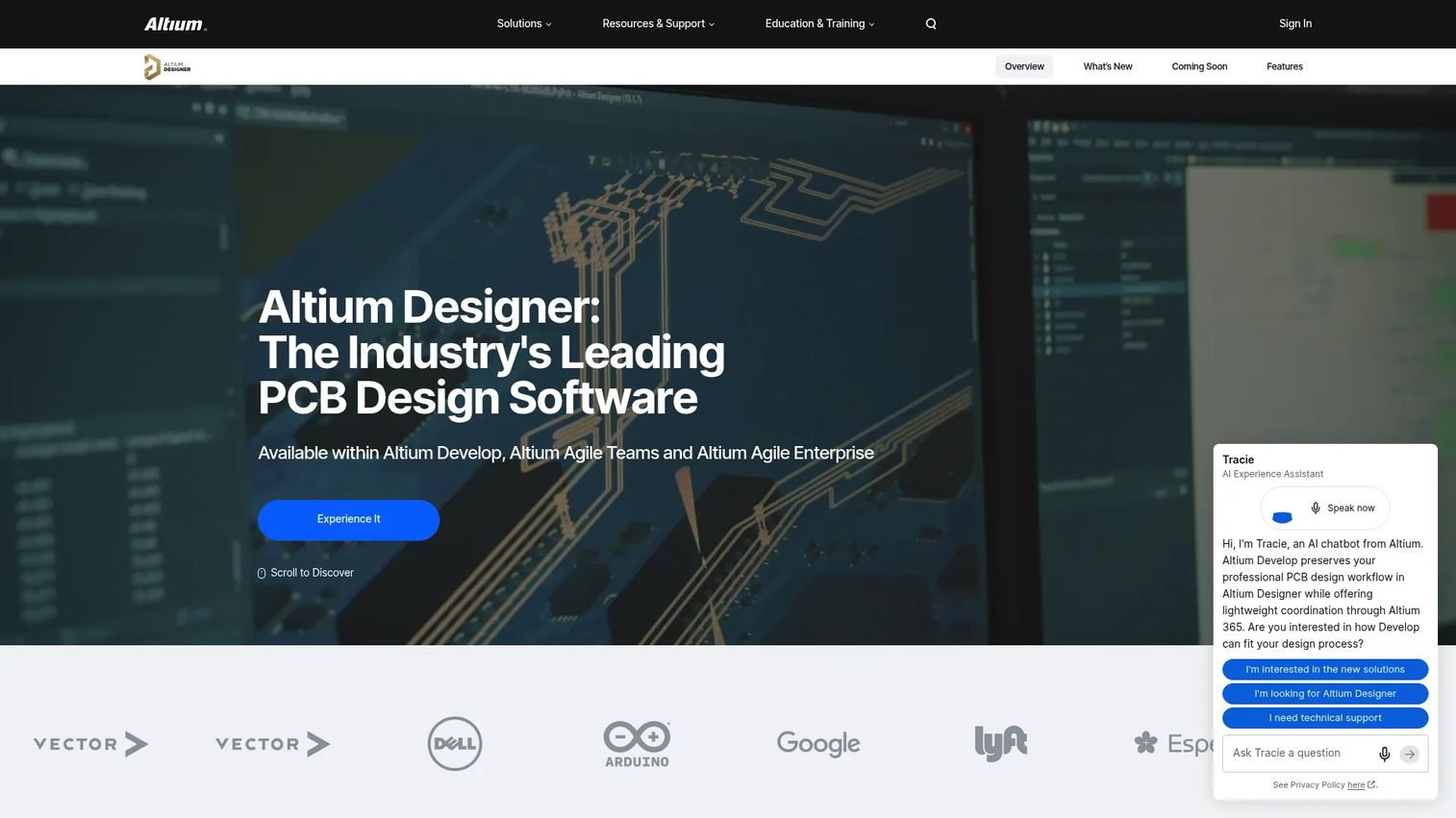
Altium Designer is a professional PCB design platform that unifies schematic capture, PCB layout, simulation, constraint management, component sourcing, and manufacturing release in one environment. It handles HDI, rigid-flex, wire bonding, multiboard, and harness design workflows. The platform connects to Altium 365 for cloud collaboration, version control, and supply-chain data.
Best for: Professional engineering teams designing complex commercial electronics who need an end-to-end PCB workflow.
Key features
- Unified schematic capture and PCB layout with shared design data
- Constraint-driven interactive routing and high-speed design tools
- SPICE simulation, power analysis, and signal-integrity analysis
- 3D PCB visualization with native MCAD integration
- Manufacturing release outputs including Gerber, ODB++, and IPC-2581
Why choose Altium Designer: It removes the fragmentation that comes from chaining together multiple tools. When the board is complex enough that a routing error or library mismatch causes a respin, having constraints, sourcing data, and design rules in one connected environment pays off.
Altium Designer pricing: Plans start at $460/month, billed annually. Trial access is available where offered by Altium sales.
2. KiCad
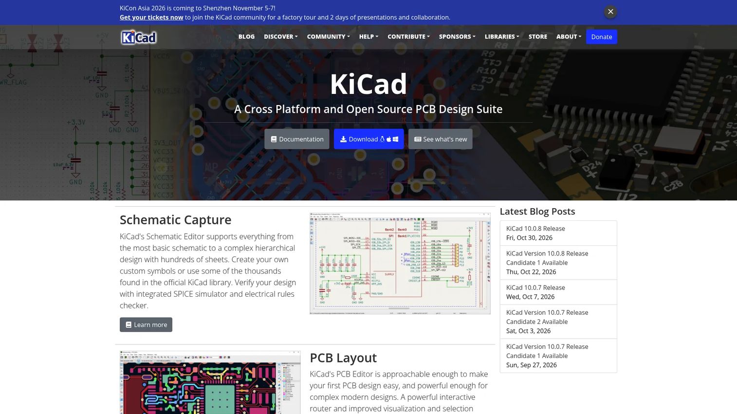
KiCad is a free, open-source, cross-platform EDA suite for schematic capture, PCB layout, simulation, and manufacturing output. It runs on Windows, macOS, and Linux under GPL-based licensing with no restrictions on commercial use. The community maintains component libraries containing symbols, footprints, and 3D models, and the project accepts optional donations to support development.
Best for: Engineers, students, and hardware teams who want capable ECAD without any license cost.
Key features
- Schematic capture with ERC and netlist export
- PCB layout with interactive routing and DRC
- Integrated SPICE simulation support
- Built-in 3D PCB viewer with realistic rendering
- Manufacturing exports including Gerber, IPC-2581, and Excellon drill files
Why choose KiCad: Free does not mean limited here. KiCad handles multi-layer boards, differential pairs, and high-density footprints well. For budget-conscious teams, students, or anyone who wants full control over tooling without vendor lock-in, it's the strongest free option available.
KiCad pricing: KiCad is free and open source. Donations support the project and are accepted through the official site.
G2 rating
4.5/5 (G2, 69 reviews)
3. EasyEDA

EasyEDA is a browser-based PCB design and circuit simulation tool that runs entirely online with optional desktop and offline modes. It combines schematic capture, PCB layout, DRC, 3D preview, Gerber export, BOM management, and component library access in a cloud environment. The platform connects directly to JLCPCB for fabrication and LCSC for component sourcing.
Best for: Engineers, makers, and students who want quick prototyping with a browser-first workflow and direct manufacturing connections.
Key features
- Browser-based schematic capture and PCB layout
- Circuit simulation with component parameter support
- Cloud project storage with team collaboration tools
- Integrated BOM and component sourcing data
- Direct Gerber export and JLCPCB manufacturing workflow
Why choose EasyEDA: The manufacturing-to-fabrication path is faster here than almost anywhere else. If your goal is getting a prototype board ordered quickly without installing software, EasyEDA removes most of the friction between design and fab submission.
EasyEDA pricing: Core features are free forever for individuals and commercial use. Paid individual plans start at $19.9/month (billed annually) for added cloud storage and priority support. Enterprise plans at $39.9/month per member are listed as coming soon.
G2 rating
4.4/5 (G2)
4. CircuitMaker

CircuitMaker is a free PCB design tool from Altium built around community sharing and open hardware collaboration. It uses Altium-style schematic and PCB design capabilities with access to component data backed by Octopart. Projects are shared publicly through Altium 365, making it well suited for open-source hardware efforts. The platform supports 16 signal layers plus 16 plane layers with no PCB dimension restrictions.
Best for: Open hardware designers, makers, and students who want Altium-style workflows on free software.
Key features
- Free schematic capture and multi-layer PCB layout
- Push-and-shove interactive routing
- Community component library with Octopart data
- Native 3D PCB visualization
- Gerber, NC Drill, and ODB++ manufacturing outputs
Why choose CircuitMaker: The combination of Altium-derived design tools and community sharing is genuinely useful for open hardware projects. Teams that need private commercial workflows should review the public-project sharing model before committing, since all projects are visible to the community.
CircuitMaker pricing: CircuitMaker is free to use. A free account is required to access the platform and community project library.
G2 rating
4.3/5 (G2, 110 reviews)
5. Autodesk Fusion Electronics

Autodesk Fusion Electronics is the PCB design environment built inside Autodesk Fusion. It delivers schematic capture, PCB layout, SPICE simulation, Gerber output, and DFM checks alongside native access to Fusion's 3D mechanical modeling tools. The ECAD-to-MCAD integration means engineers can push board geometry directly into the enclosure design and check clearances without exporting files between platforms.
Best for: Product development teams designing PCBs inside a mechanical product where enclosure fit and 3D integration matter.
Key features
- Schematic capture with ERC and component management
- PCB layout and routing with DRC
- SPICE simulation support
- MCAD-ECAD 3D co-design and enclosure clearance checking
- Gerber, drill files, and assembly output generation
Why choose Autodesk Fusion Electronics: The mechanical integration is the differentiator. If your hardware team already uses Autodesk Fusion for enclosure design, keeping the PCB in the same environment removes the back-and-forth between ECAD and MCAD tools. It works best when board and product design happen in parallel, not sequentially.
Autodesk Fusion Electronics pricing: Autodesk Fusion plans start at $680/year (annual billing) or $85/month. A 3-year subscription is available at $2,040. PCB capabilities are included in the standard Fusion subscription.
G2 rating
4.5/5 (G2, Autodesk Fusion)
6. Cadence OrCAD X

Cadence OrCAD X is a professional PCB design platform covering schematic capture, PCB layout, PSpice simulation, constraint management, BOM and supply-chain intelligence, and manufacturing preparation. Three tiers, Standard, Professional, and Professional Plus, scale capability from core schematic-to-layout workflows up to advanced simulation, high-speed analysis, and Simulink integration. Both 30-day commercial and 6-month academic trials are available.
Best for: Small and midsize engineering teams that need an integrated PCB design, simulation, and manufacturing workflow with a path into Cadence's broader EDA stack.
Key features
- Schematic capture and full PCB layout editor
- Integrated PSpice circuit simulation
- Constraint manager for high-speed routing rules
- Live BOM and supply-chain intelligence
- 3D visualization and MCAD co-design support
Why choose Cadence OrCAD X: The Standard tier entry price makes it accessible for teams that want Cadence's simulation and constraint depth without the full enterprise commitment. As team complexity grows, upgrading to Professional or Professional Plus is a logical path rather than a platform change.
Cadence OrCAD X pricing: OrCAD X Standard starts at $1,280/year (annual billing). Professional and Professional Plus tiers are available through Cadence sales. A 30-day commercial trial is offered.
G2 rating
4.2/5 (G2, OrCAD seller profile)
7. Cadence Allegro X

Cadence Allegro X is Cadence's enterprise PCB and system design platform for high-speed, high-density, and complex multi-domain electronic systems. It combines concurrent team design with real-time collaboration, advanced timing and signal-integrity analysis, power-integrity analysis, HDI and rigid-flex support, and AI-powered routing assistance for component placement and critical-net routing. Library management, version control, and supply-chain data are built into the same environment.
Best for: Enterprise hardware teams running high-speed, high-density PCB designs where electrical performance, constraint depth, and team-scale design control are non-negotiable.
Key features
- Concurrent team PCB design with real-time shared data
- High-speed analysis: Timing, length, phase, signal integrity, power integrity
- AI-powered component placement and critical-net routing
- HDI, rigid-flex, and 3D MCAD co-design support
- Integrated version control, library management, and supply-chain insights
Why choose Cadence Allegro X: The investment is justified when design complexity, electrical performance margins, and multi-engineer concurrency make simpler tools a liability. For presales engineers supporting Cadence customers, Allegro X is where the enterprise differentiation conversation happens: Analysis depth, constraint coverage, and AI acceleration versus the cost and deployment overhead.
Cadence Allegro X pricing: Pricing is through Cadence sales. Ask for seat counts, module selections, and analysis add-ons to get an accurate quote.
G2 rating
4.3/5 (G2, Cadence Design Systems)
8. Siemens Xpedition

Siemens Xpedition is a scalable enterprise PCB and electronic systems design platform built for organizations ranging from independent engineers to large global teams. It covers systems architecture, advanced PCB layout automation, design reuse, verification, simulation, manufacturing data management, and ECAD-MCAD collaboration. The platform scales across product complexity tiers, making it one of the more flexible enterprise options for organizations with mixed-complexity design portfolios.
Best for: Large electronics organizations where PCB design connects to enterprise engineering, manufacturing, and PLM systems.
Key features
- Enterprise PCB layout with advanced automation tools
- Design reuse and configuration management
- Integrated verification and simulation workflows
- ECAD-MCAD collaboration and 3D co-design
- Manufacturing data output and process management
Why choose Siemens Xpedition: It fits best when PCB design is one component of a broader electronic product architecture, and when engineering, manufacturing, and lifecycle management systems must stay connected. Teams already using Siemens' broader digital industry portfolio will find the integration straightforward.
Siemens Xpedition pricing: Pricing is through Siemens EDA sales. Contact Siemens for current packaging, evaluation options, and partner pricing.
9. Siemens PADS Professional
Siemens PADS Professional is a professional PCB design suite for hardware engineers and small workgroups. It covers schematic capture, PCB layout, constraint-driven routing automation, analog and mixed-signal simulation, signal-integrity analysis, RF design, and design-for-manufacturing checks. Rigid-flex PCB design and electro-mechanical co-design are included.
Best for: Small and midsize engineering teams that need professional PCB design depth, including rigid-flex and RF support, without the overhead of a full enterprise platform.
Key features
- Schematic capture and constraint-driven PCB layout
- Routing automation for complex board topologies
- Rigid-flex PCB design support
- Analog/mixed-signal simulation and signal-integrity analysis
- DFM checks and manufacturing output generation
Why choose Siemens PADS Professional: It occupies a practical middle ground between entry-level tools and full enterprise deployments. Teams outgrowing tools like KiCad or DipTrace but not ready for Xpedition will find PADS Professional covers most professional design requirements, including analysis capabilities that many commercial desktop tools leave out.
Siemens PADS Professional pricing: Pricing is through Siemens EDA sales. Contact Siemens for current packaging and evaluation options.
G2 rating
4.1/5 (G2, PADS Professional)
10. Zuken CR-8000
Zuken CR-8000 is an enterprise PCB and electronic system design platform for complex hardware products. It handles PCB subsystem architecture planning, 2D and 3D multi-board PCB design, chip/package/board co-design, signal-integrity and power-integrity analysis, EMC analysis, design-for-manufacturing checks, and manufacturing output generation. Library and design data management are integrated throughout the workflow.
Best for: Enterprise engineering teams designing complex multi-board electronic products where architectural planning, co-design, and analysis must work together.
Key features
- PCB subsystem architecture design and verification
- 2D and 3D multi-board PCB design with MCAD integration
- Chip, package, and board co-design
- Signal integrity, power integrity, and EMC analysis
- DFM checks and manufacturing output generation
Why choose Zuken CR-8000: The product-centric design approach is distinctive. Rather than treating each board in isolation, CR-8000 builds from the electronic product architecture down, which suits complex systems where multi-board topology and chip-package-board interactions drive design decisions. The 5.0/5 G2 rating, while based on a small sample, reflects strong satisfaction among verified users.
Zuken CR-8000 pricing: Pricing is through Zuken sales. Contact Zuken for current module options and evaluation terms.
G2 rating
5.0/5 (G2, CR-8000 Design Force, 3 reviews)
11. DipTrace
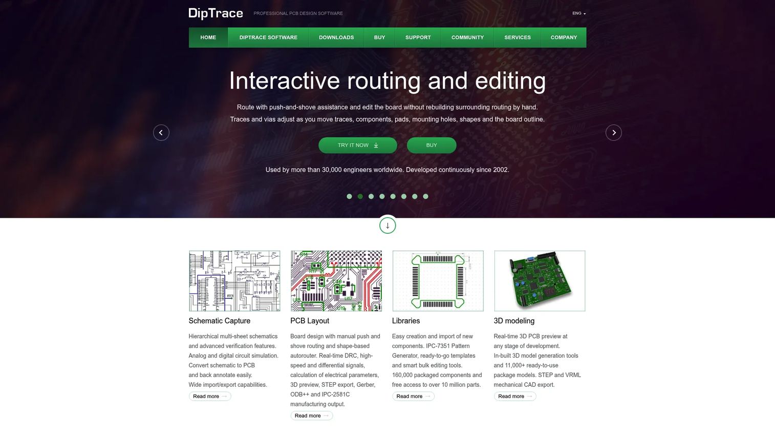
DipTrace is professional PCB design software for engineers who want schematic-driven, multilayer PCB design with a perpetual license model and no recurring subscription fees. It covers hierarchical multi-sheet schematic capture, interactive push-and-shove routing, shape-based autorouting, real-time DRC, high-speed differential-pair support, and 3D PCB preview with STEP export. Manufacturing outputs include Gerber, ODB++, and IPC-2581C. A free edition is available with a 300-pin and 2-layer limit.
Best for: Independent engineers and small hardware teams who want professional PCB design depth with perpetual licensing and no annual subscription.
Key features
- Hierarchical multi-sheet schematic capture
- Interactive push-and-shove routing with shape-based autorouting
- Real-time DRC and differential-pair routing support
- 3D PCB preview with STEP export
- Gerber, ODB++, and IPC-2581C manufacturing outputs
Why choose DipTrace: The perpetual license model is the standout for teams wary of annual subscription costs. A one-time purchase covers the software indefinitely, and the tier structure, from Starter at $75 to Full at $995, makes it budget-accessible across team sizes.
DipTrace pricing: Perpetual licenses range from $75 (Starter) to $145 (Lite), $395 (Standard), $695 (Extended), and $995 (Full). No recurring fees apply. A free edition covers up to 300 pins and 2 signal layers.
G2 rating
4.3/5 (G2)
12. LibrePCB
LibrePCB is a free, open-source, cross-platform EDA suite designed around usability and structured library management. It covers schematic editing with multi-page schematics, live ERC, assembly data management, and EAGLE project import. The PCB board editor handles multi-layer design, blind and buried vias, DRC, and a live 3D viewer. Output jobs cover Gerber/Excellon, pick-and-place files, BOM, IPC-D-356A netlists, STEP, PDF, and SVG. The official site states there are no costs, restrictions, or limitations.
Best for: Beginners, makers, and open-source users who want a clean, usable PCB design workflow for simpler boards.
Key features
- Multi-page schematic editor with live ERC
- Multi-layer PCB editor with DRC and integrated 3D viewer
- Blind and buried via support
- EAGLE project import
- Gerber/Excellon, BOM, pick-and-place, STEP, and IPC-D-356A outputs
Why choose LibrePCB: The library structure is noticeably cleaner than older open-source tools, which reduces the time spent managing symbol and footprint inconsistencies. For someone starting with printed circuit board design or building simple boards, LibrePCB offers a low-friction entry point without the configuration overhead that older tools require.
LibrePCB pricing: LibrePCB is completely free and open source with no usage restrictions.
Considerations when choosing pcb design software
Match the tool to board complexity
A two-layer prototype and a 20-layer high-speed rigid-flex product need different tooling. Check whether the tool supports your target layer count, blind and buried vias, impedance control, HDI structures, and differential-pair routing constraints before committing. Enterprise tools handle all of these by design; free tools handle some and not others.
Check schematic and library quality
Symbol and footprint accuracy is where design errors start. Evaluate whether the tool provides verified component libraries, supports custom symbols and footprints, offers footprint validation tools, and maintains versioning on library updates. Poor library management creates downstream PCB layout errors that are expensive to catch after fabrication.
Validate routing, rules, and analysis
DRC and ERC are baseline requirements, not differentiators. The real question is depth: Does the tool support signal-integrity simulation, power-integrity analysis, and impedance management? For analog, RF, and high-speed designs, these capabilities reduce board respins. For simpler digital boards, DRC and basic ERC may be enough.
Review collaboration and release workflow
If more than one engineer touches the design, check how the tool handles concurrent editing, version control, and design review permissions. Manufacturing release workflows matter too: Can you generate a complete release package with BOM, Gerber, assembly drawings, and change documentation from one place?
Confirm manufacturing and sourcing outputs
Verify that the tool exports the formats your fabricator accepts. Most manufacturers work with Gerber or Gerber X2, Excellon drill files, and pick-and-place data. Some require ODB++ or IPC-2581. BOM export format affects how procurement and contract manufacturers receive component data. Check requirements before finalizing your tool choice.
Conclusion
For most professional engineering teams, Altium Designer remains the strongest all-around commercial option when board complexity, supply-chain integration, and manufacturing release control matter. KiCad is the clear answer for anyone who needs capable ECAD at no cost, and it handles more than most engineers expect from a free tool. EasyEDA wins on speed-to-prototype for browser-first workflows, and CircuitMaker offers a useful on-ramp for open hardware projects.
Teams working on mechanical-electronic products should look closely at Autodesk Fusion Electronics for its ECAD-MCAD integration. Engineering organizations running complex, high-speed designs with multi-person teams will find the right fit among Cadence Allegro X, Siemens Xpedition, Siemens PADS Professional, and Zuken CR-8000. For independent engineers who prefer perpetual licenses, DipTrace hits a practical price point. For learners and open-source contributors, LibrePCB is a solid, unrestricted starting point.
If you're exploring how to present complex technical products like EDA software to buyers, see how 3D visualization software, additive manufacturing software, and CAD/CAM software are evaluated across similar technical categories on the Guideflow blog.
FAQs
KiCad, EasyEDA, CircuitMaker, DipTrace, and LibrePCB all work well as starting points. KiCad offers the most complete free desktop experience for someone who wants to build real skills. EasyEDA removes the installation step entirely and connects directly to fabrication. DipTrace's Starter edition costs $75 for a perpetual license if you want a paid tool with a low entry point.
KiCad is the strongest general-purpose free option. It handles multi-layer boards, SPICE simulation, 3D visualization, and Gerber output at no cost, with no commercial-use restrictions. CircuitMaker and LibrePCB are solid alternatives for open hardware community work and simpler boards respectively.
For prototyping, collaboration, and manufacturing-connected workflows, yes. EasyEDA handles designs that many professional teams would be comfortable sending to fabrication. Where online tools typically fall short is in enterprise constraints: Access control, version control depth, advanced simulation, and design data governance. For regulated environments or teams with strict data requirements, a desktop or enterprise tool is the more defensible choice.
Core requirements are schematic capture, PCB layout, interactive routing, component libraries, DRC, ERC, 3D visualization, BOM export, and manufacturing file generation. Teams working on analog, power, or high-speed boards should add SPICE simulation and signal-integrity analysis to that list. Enterprise teams need version control, permission management, and PLM integration on top of those basics.
ECAD (electronic computer-aided design) is the broader category for all software used to design electronic systems, including IC design, packaging, and system architecture tools. PCB design software is a focused subset of ECAD: It handles printed circuit board schematic capture, physical layout, validation, and manufacturing output workflows specifically.
Simulation matters most for analog circuits, power supplies, RF designs, and high-speed digital boards where signal behavior before physical layout is uncertain. For straightforward digital boards with well-characterized components, DRC and ERC may be sufficient without dedicated SPICE simulation. Most professional tools include simulation; free tools like KiCad support it through SPICE integration.
Most fabricators require Gerber or Gerber X2 files for copper layers, Excellon drill files, a pick-and-place file for assembly, a BOM, and assembly drawings. Some manufacturers accept ODB++ or IPC-2581 as a complete alternative to a Gerber set. Check the specific fabricator's requirements before generating your release package, since formats vary by vendor.
Altium Designer, Cadence Allegro X, Siemens Xpedition, Siemens PADS Professional, and Zuken CR-8000 are the enterprise-grade options. The right choice depends on design complexity, team size, and which analysis capabilities are required. Cadence Allegro X suits high-speed and high-density boards with strong AI-assisted routing. Siemens Xpedition fits organizations where PCB design must integrate with broader enterprise engineering and PLM systems. Zuken CR-8000 excels at multi-board product architecture with chip/package/board co-design.